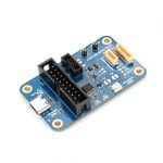

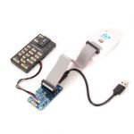


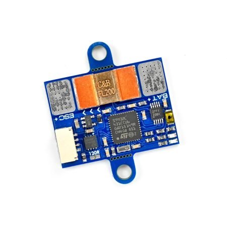
The Pixhawk Debug Adapter provides a JTAG SWD and Serial interface to debug Pixhawk compatible hardware. Both the Target 6-pin (FMUV5) and Target 10-pin (FMUVxX) Pixhawk debug connector standards are supported.
The built-in FTDI serial interface eliminates the need for a separate FTDI cable. The interface is specially designed to not backfeed the FMU, thus ensuring stable and reliable debugging regardless of power sequencing.
Two Host JTAG interface standards are supported: The 10-pin ARM compatible with the Segger Jlink-mini and 20-pin compatible with the Segger Jlink or STLink.
The adapter also provides easily accessible ground points. When used with the 10-pin target cable it further supports two GPIO from the CPU that can be used to perform accurate signal timing. Target Reset via a push button, JTAG or optionly RTS from the serial interface is also supported over the 10-pin target interface.
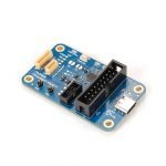
Jumperable Options:
JP1 – Normally Open. Soldering this part will bypass the RXD_DEBUG Back-feeding protection diode. This should not be needed unless the target already has the Back-feeding protection diode AND the target is not receiving data due to signaling levels.
JP2 – Normally Open. Soldering this part will connect the RTS signal from the HOST to the CPU nRST line. With this jumper soldered, the CPU nRST will be wired OR of the reset Button, the JTAG reset and the HOST RTS line. With it open the HOST RTS line is not connected. This could be used on automated test racks.
Block Diagram

Only logged in customers who have purchased this product may leave a review.


Reviews
There are no reviews yet.